The Most Useful Semiconductor Paper I Wrote This Year Says Don't Buy It
A defensive due-diligence memo on LogicFolding, 3D stacking, and why the math is the easy part

Six probabilities multiplied together. That is the entire investment thesis for LogicFolding-style 3D logic stacking, and on May 27, 2026, I closed my third red-team pass on the idea with every one of those probabilities flagged red.
The paper sits in my repo now as a 16-page no-action decision memo. Final line: *Do not trade. Do not allocate. Do not treat as a viable alternative to backside power or conventional 3D packaging.* I am posting about it because the most underrated genre in semiconductor writing is the one where someone explains, with receipts, why the thing on the press release does not work yet.
The thing on the press release
Huawei announced something they call Tau Scaling. Reuters covered it the same week as the Intel 18A and TSMC A16 rollouts. The framing, repeated across analyst notes and venture pitch decks, was that critical-path wiring could be folded vertically into a stacked-die structure and that this would substitute, at least partly, for advanced-node lithography. If that were true at production volume, the implications for capex allocation across foundries, EDA vendors, and chiplet integrators would be enormous. Tens of billions of dollars of positioning hangs on whether the claim is what it appears to be.
Maybe it is. The public evidence package does not exist, and the equation you would need to actually test it has a load-bearing term that almost every popular treatment quietly drops.
The term that does not get dropped
Here is the path-level break-even inequality. If you fold a horizontal wire of length ℓ_h into the vertical dimension, the delay you save has to clear the delay you spend on vias and bond contacts:
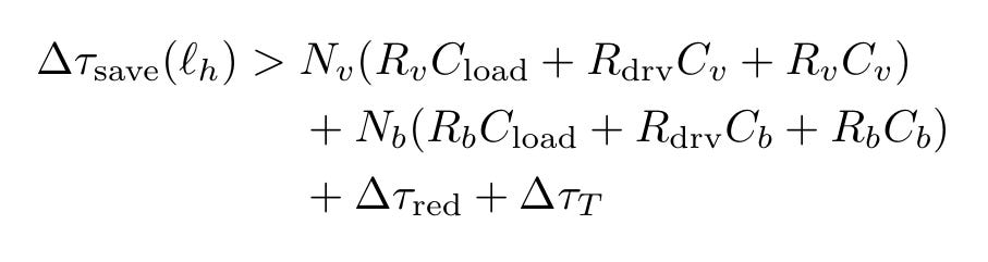
Most slides you will see compress this to the first two terms inside each parenthesis. Driver pushing the contact, contact pushing the load. Two RC products, clean linear scaling in number of vias.
The third term in each parenthesis is the half-Elmore self-loading of the via or bond itself: R_v · C_v and R_b · C_b. They are quadratic in the contact’s own parasitic, and at advanced nodes they are not negligible. They are the term that flips otherwise-positive break-evens negative once you measure rather than assume. Call it the dropped-term gap.
Drop them, and the math says fold every wire. Keep them, and the math says fold a small subset of long global wires and pay area, yield, and thermal penalties to do so. Those are the two different worlds the press release lets you live in.
The dropped-term gap is the single most common analytical failure in 3D-stacking optimism. If a deck does not show you the self-loading term, the analyst writing it does not know it should be there, or knows and decided you should not.
Why the rest of the gates are also red
The break-even inequality is one gate. The honest decision model multiplies six:

G_0 is the business partnership giving you access to a foundry that will run dual-active-logic test vehicles with auditable data rights. G_P is parasitic break-even on real silicon. G_T is thermal viability under sustained workloads (not burst benchmarks). G_Y is yield, DFT coverage, and DPPM. G_E is a reproducible EDA flow. G_C is sustained performance-per-watt-per-cost-per-good-die beating the planar alternative.
Each conditional is close to zero today. Multiply six near-zeros and you get a near-zero. A press release moves one term. An investment decision needs all six.
The memo’s stop-light table marks every category red except “research interest,” which is yellow. I do not think this is a controversial conclusion among people who have built advanced packaging. I think it is unusual to see it written down with the equations attached.
Defensive due diligence as a product
The job here is defensive due diligence: keeping a portfolio manager, an engineering VP, or a board from allocating against a thing that does not exist yet, before the press release wave teaches them it does.
The institutional buy-side has plenty of optimistic sell-side coverage. What it lacks is one technical reader who will read the spec sheet, work out the parasitic budget, identify the term that got dropped, and write the no-action memo.
It is the call you make at 6 p.m. on a Friday, after the analyst note drops: the equation in their appendix is missing a term, here is which one, here is why it matters, do not move size on this until Monday. That call is the product.
The deliverable is the conditions under which the answer would change. Yes-or-no falls out of those conditions on its own.
In this case there are three:
1. A shipping product is torn down and shown to contain folded active logic, with measured sustained thermal and path-time behavior.
2. A foundry or integrated manufacturer publicly commits to dual-active-logic stacking with disclosed or escrowed data access.
3. An open reference flow demonstrates reproducible 3D partitioning and proxy signoff on a public PDK (SkyWater 130 nm, GF180), so the methodology has executable content rather than only operator notation.
None of those exist today. Until one does, every press cycle on this topic should be filed under “interesting research, not allocation thesis.”
The open reference flow as calling card
I scaffolded the third trigger this morning. A Python orchestrator that evaluates the full break-even inequality (with the self-loading term restored), a Rust crate that vectorizes the path evaluation across hundreds of thousands of mock paths under rayon, and a Julia module that runs the FFT thermal convolution and the EWMA run-to-run controller with variable metrology delay. The whole repo is licensed permissively and points at public PDKs.
The code lives at logic-folding-reference-flow. The memo it implements is bundled in the same repo under `docs/`.
This methodology cannot prove feasibility. The memo is explicit: an open flow on SkyWater 130 nm tells you the methodology is coherent. It does not tell you it works at 5 nm-class active logic. The latter still requires foundry data and silicon.
But it does something the press cycle cannot. It makes the claim falsifiable. Anyone who wants to argue with the math has to argue with the code. Anyone who wants to disagree with the no-action conclusion can fork the repo, change the parasitic assumptions, and show me a regime where the inequality flips. That is the cleanest peer review I know how to run as an independent researcher with no corporate red-team to bounce off.
What I want from a reader
If you are at a hedge fund or a venture fund and you are positioning on this narrative, the test I would run before adding exposure is the one in the memo’s table 4. Find the evidence column you are pricing in, and ask whether it is a press release, a roadmap, a private demo, a named foundry shuttle, an open reference flow, a teardown, or a teardown with positive perf-per-watt-per-dollar. Each row gets a different decision. The first three get NO.
If you write for one of the deeply technical semi-analysis publications, the dropped-term gap is the kind of pattern that travels. Treat it as a class of analytical failure rather than a one-time observation, and look for it in any future stacking, photonics, or chiplet pitch that promises substitution for lithography scaling.
If you run an engineering team and someone on it is excited about LogicFolding-class techniques, the question worth asking is, “What set of paths in our actual netlist would clear the gate under measured rather than assumed parasitics?” Feasibility is the wrong abstraction layer. The answer is almost always “long global wires only,” and that puts the technique in the floorplanning category, not the scaling-law category.
Where this goes
The memo and the reference flow are both public, in the same repository, under Apache-2.0. The partitioning logic and the parasitic break-even inequality both have something to bind against, and the equations cite their memo sections by number.
If the open flow turns into the third reopen trigger by virtue of being the only one anyone has actually built, that is fine with me. A no-action memo exists to put the conditions under which the action would change into print. When those conditions arrive, the response is fast and disciplined rather than narrative-driven.
This is my first time hearing that you can stack logic transistors on top of each other, so I'm kind of interested to see how this technology pans out (or if it /does/ pan out). Usually, chips are designed using laser lithography, which essentially burns away part of a chip and prints silicon in the newly-blasted trenches. At least this is how they've been making them for decades.
Obviously the major drawback to this is that you can't really "stack" transistors on top of each other without physically stacking the wafers. Put simply, a laser can only blast away the surface of a wafer, so how could it create multiple layers? I think that's the part I'm missing, so I'll need to read more on how they mass-manufacture something like this!
I think put even more simply, this breakthrough is enticing because if you stack transistors, it's like taking an elevator to another floor instead of walking to a different office across the street (and since electricity is literally limited by the speed of light, then theoretically reducing the distance between transistors could increase the clock speed).
As you said, in practice the technology is going to need more time to mature, so I'm interested in reading more about this as more is developed.